| CPC H01L 21/30625 (2013.01) [H01L 21/3065 (2013.01); H01L 21/763 (2013.01); H01L 21/76224 (2013.01); H01L 28/40 (2013.01)] | 20 Claims |
|
1. A method of fabricating an integrated circuit (IC), comprising:
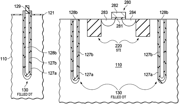
forming a layer stack on a substrate, the layer stack comprising silicon nitride layer on a first silicon oxide layer, with a second silicon oxide layer on the silicon nitride layer, the substrate comprising a semiconductor material having a top surface;
etching through the layer stack to form at least one trench into the semiconductor material;
forming a dielectric liner on sidewalls and on a bottom of the trench;
forming a polysilicon layer on the dielectric liner, wherein the polysilicon layer fills the trench and extends over the top surface;
performing a chemical mechanical planarization (CMP) process stopping on the silicon nitride layer to remove the polysilicon layer and the second silicon oxide layer to form a trench structure having a polysilicon fill;
after the CMP processing, thermally oxidizing the polysilicon layer to form a fill silicon oxide layer having a bottom surface above the top surface of the substrate; and
after forming the fill silicon oxide layer, removing the silicon nitride layer and the fill silicon oxide layer, thereby exposing the polysilicon fill.
|