| CPC H01L 21/30621 (2013.01) [H01L 21/3065 (2013.01); H01L 21/30604 (2013.01); H01L 21/32136 (2013.01); H01L 21/32138 (2013.01); B81C 2201/0136 (2013.01); H01L 21/308 (2013.01)] | 7 Claims |
|
1. A semiconductor device manufacturing method comprising the steps of:
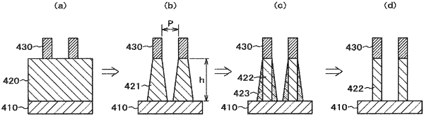
etching a semiconductor material formed on a substrate to have a trapezoidal shape in a cross-section view using a plasma;
forming a damage layer in an etched sidewall linear tapered portion of the semiconductor material which has the trapezoidal shape in the cross-section view, wherein the damage layer is formed on a surface of the substrate and does not extend into a material forming the substrate; and
removing the damage layer.
|