| CPC H01L 21/02499 (2013.01) [H01L 21/0262 (2013.01); H01L 21/02381 (2013.01); H01L 21/02433 (2013.01); H01L 21/02639 (2013.01); H01L 29/0603 (2013.01)] | 16 Claims |
|
1. A process for the hetero-integration of a semiconductor material of interest on a silicon substrate, comprising:
a step of removing a native oxygen from the silicon substrate;
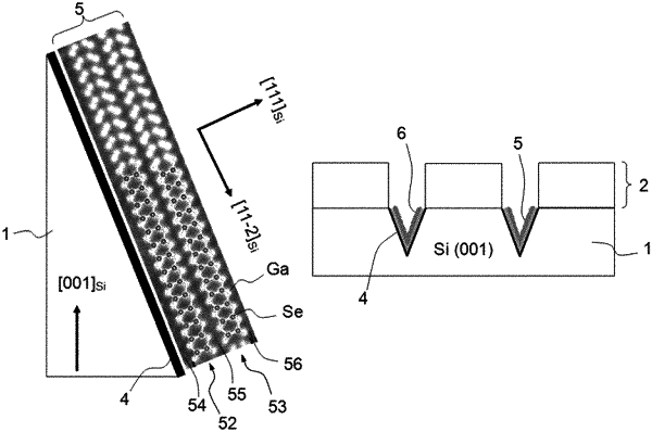
a step of structuring the substrate which comprises a step of producing a growth mask on the surface of the silicon substrate, said growth mask comprising a plurality of masking patterns, two masking patterns being separated by a trench wherein the silicon substrate is exposed;
a step of forming a two-dimensional buffer layer made of a 2D material, said buffer layer being free of side bonds on its free surface and being formed selectively on a silicon plane of [111] orientation in at least one trench, said step of forming a buffer layer being performed after the structuring step and being performed by an organometallic vapour deposition (MOCVD) technique;
a step of forming at least one layer of a semiconductor material of interest on the buffer layer; and
a passivation step which consists in depositing an atomic biplane of gallium and selenium onto the silicon plane of [111] orientation so as to form a silicon-gallium-selenium passivated surface on said plane.
|