| CPC H01L 21/02115 (2013.01) [H01L 21/31111 (2013.01)] | 20 Claims |
|
1. A semiconductor processing method comprising:
etching one or more features partially through a dielectric material to expose material from one or more layer pairs in a plurality of layer pairs formed on a substrate;
halting the etching prior to penetrating fully through the dielectric material, and prior to exposing material from one or more remaining layer pairs in the plurality of layer pairs formed on the substrate;
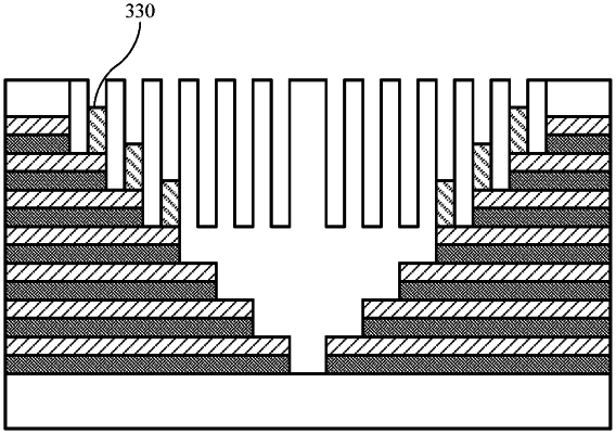
after halting the etching and exposing the material from the one or more layer pairs, and before exposing the material for the one or more remaining layer pairs, forming a layer of carbon-containing material on the exposed material from each of the one or more layer pairs having exposed material; and
after forming the layer of carbon-containing material, etching the one or more features fully through the dielectric material to expose material for each of the one or more remaining layer pairs formed on the substrate.
|
|
12. A semiconductor processing method comprising:
etching one or more features partially through a dielectric material to expose silicon nitride from a first set of layer pairs formed on a substrate;
halting the etching prior to penetrating fully through the dielectric material, and prior to exposing a second set of layer pairs formed on the substrate under the first set of layer pairs;
after halting the etching and exposing the silicon nitride from the first set of layer pairs, and before exposing the second set of layer pairs, forming a layer of carbon-containing material on each region of silicon nitride exposed on the first set of layer pairs; and
after forming the layer of carbon-containing material, etching the one or more features fully through the dielectric material to expose silicon nitride from the second set of layer pairs formed on the substrate.
|
|
19. A semiconductor processing method comprising:
etching one or more features partially through a dielectric material to expose silicon nitride from a first set of layer pairs formed on a substrate, wherein the first set of layer pairs are formed in a staircase structure, and wherein each feature of the one or more features is aligned with a separate layer pair in the first set of layer pairs;
halting the etching prior to penetrating fully through the dielectric material, and prior to exposing a second set of layer pairs formed on the substrate under the first set of layer pairs;
after halting the etching and exposing the silicon nitride from the first set of layer pairs, and before exposing the second set of layer pairs, forming a layer of carbon-containing material on each region of silicon nitride exposed on the first set of layer pairs; and
after forming the layer of carbon-containing material, etching the one or more features fully through the dielectric material to expose silicon nitride from the second set of layer pairs formed on the substrate.
|