| CPC H01J 37/244 (2013.01) [G01N 23/2251 (2013.01); H01J 37/28 (2013.01); H01J 2237/2448 (2013.01); H01J 2237/24585 (2013.01); H01J 2237/2806 (2013.01); H01J 2237/2813 (2013.01)] | 13 Claims |
|
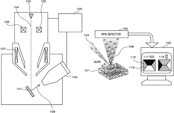
1. A scanning electron microscope for evaluating a strain in a sample, the scanning electron microscope comprising:
a spin detector configured to measure secondary electron spin polarization of secondary electrons emitted from the sample; and
an analysis device configured to analyze secondary electron spin polarization data measured by the spin detector, wherein
the analysis device evaluates the strain in the sample by calculating a difference in the secondary electron spin polarization data of adjacent pixels.
|