| CPC H01G 9/08 (2013.01) [H01G 9/048 (2013.01); H01G 9/15 (2013.01); A61N 1/05 (2013.01); H01G 9/0425 (2013.01)] | 10 Claims |
|
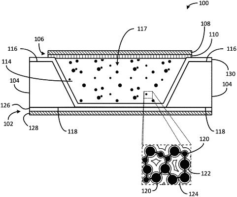
1. An electrical component comprising:
a substrate comprising:
a first major surface;
a second major surface; and
a cavity disposed in the substrate and extending between the first major surface and the second major surface;
an anode electrode comprising a conductive foil layer disposed on the second major surface of the substrate and over the cavity;
tantalum material disposed within the cavity and comprising tantalum particles;
a dielectric layer disposed on the tantalum particles;
an electrolyte cathode layer disposed on the dielectric layer; and
a cathode electrode disposed over the cavity.
|