| CPC G11C 16/0483 (2013.01) [G11C 5/063 (2013.01); G11C 7/06 (2013.01); G11C 16/08 (2013.01); G11C 16/26 (2013.01); H01L 23/528 (2013.01); H01L 23/5226 (2013.01); H10B 43/10 (2023.02); H10B 43/27 (2023.02); H10B 43/35 (2023.02); H10B 43/40 (2023.02)] | 17 Claims |
|
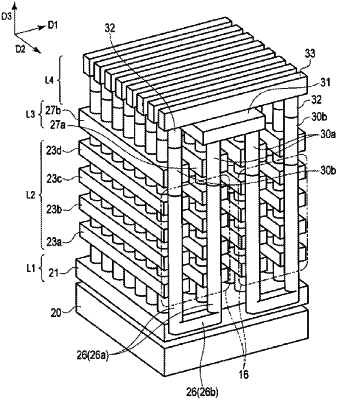
1. A semiconductor storage device, comprising:
a plurality of word lines extending in a first direction and a second direction, and separated from each other in a third direction, the first, second, and third directions crossing one another;
a plurality of sense amplifier circuits partially overlapping the word lines when viewed in the third direction;
a plurality of memory strings intersecting the word lines, and extending in the third direction;
a plurality of first bit lines extending in the first direction and separated from each other in the second direction;
a plurality of second bit lines between the word lines and the sense amplifier circuits in the third direction, and extending in the first direction; and
a plurality of contact plugs extending in the third direction, respectively connected connecting the first bit lines and the second bit lines, and arranged such that one of the a first contact plug of the plurality of contact plugs, which is between second and third contact plugs of the plurality of contact plugs in the second direction, is offset with respect to the second and third contact plugs in the first direction.
|