| CPC G11C 13/0069 (2013.01) [G11C 11/161 (2013.01); G11C 13/004 (2013.01); G11C 13/0026 (2013.01); G11C 13/0028 (2013.01); G11C 13/0064 (2013.01); H10N 70/20 (2023.02); G11C 2213/79 (2013.01)] | 9 Claims |
|
1. A variable resistance memory device comprising:
a plurality of first conductors extending in a first direction and spaced from each other in a second direction intersecting the first direction;
a plurality of second conductors extending in the second direction and spaced from each other in the first direction;
a plurality of third conductors extending in the first direction and spaced from each other in the second direction;
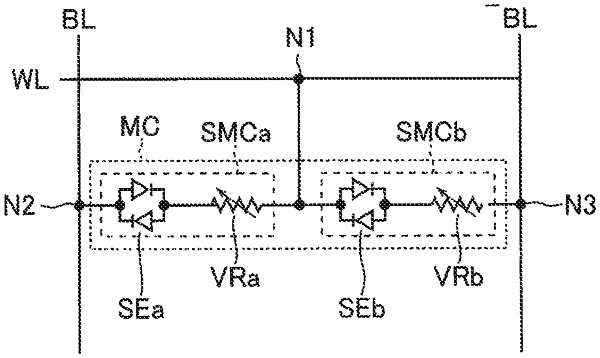
a plurality of memory cells, each memory cell being between one first conductor and one third conductor in a third direction orthogonal to the first and second directions, and each memory cell comprising:
a first sub memory cell between the one first conductor and one second conductor, the first sub memory cell including a first variable resistance element and a first bidirectional switching element; and
a second sub memory cell between the one second conductor and the one third conductor, the second sub memory cell including a second variable resistance element and a second bidirectional switching element; and
a write circuit configured to write data to one selected memory cell and output a first potential, a second potential different from the first potential, and a third potential having a magnitude between magnitudes of the first potential and the second potential,
wherein:
the first potential is applied to the one first conductor and the one third conductor of the one selected memory cell,
the second potential is applied to the one second conductor of the one selected memory cell, and
the third potential is applied to the first and third conductors of non-selected memory cells.
|