| CPC G11C 11/44 (2013.01) [H10N 60/30 (2023.02); H10N 70/253 (2023.02); B82Y 10/00 (2013.01); B82Y 25/00 (2013.01)] | 17 Claims |
|
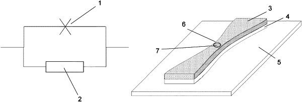
1. A memory device comprising:
a switchable resistive element comprising an active material, the active material being switchable, by current injection, between first and second values of electrical resistivity ρ1 and ρ2 at the same temperature, wherein ρ1 is different to ρ2; and
a superconductor element connected electrically in parallel with the switchable resistive element, the superconductor element being operable so that at least part of the superconductor element is switchable from a superconducting state to a non-superconducting state,
wherein the memory device is operable so that, when the superconductor element is switched from the superconducting state to the non-superconducting state, a current injection is provided through the switchable resistive element capable of switching the switchable resistive element between said first and second values of electrical resistivity.
|