| CPC G11C 11/2273 (2013.01) [G11C 11/221 (2013.01); G11C 16/0483 (2013.01); G11C 16/28 (2013.01)] | 25 Claims |
|
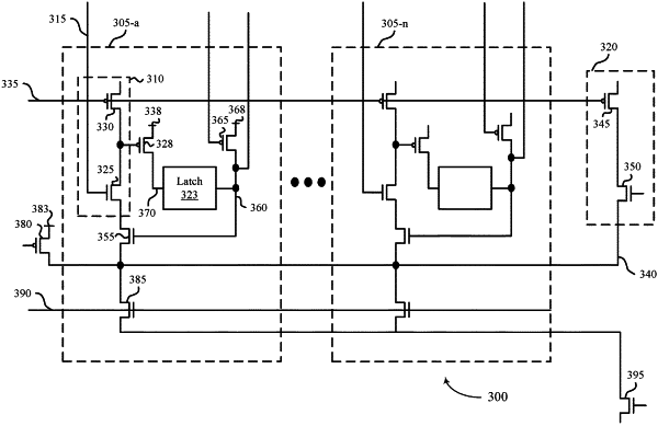
1. An apparatus, comprising:
a memory cell;
a sense amplifier coupled with the memory cell via a digit line, the sense amplifier comprising:
a latch;
a first transistor having a gate coupled with the digit line, wherein a first state of the latch couples the first transistor with a first node and a second state of the latch decouples the first transistor from the first node;
a second transistor having a gate coupled with a first bias voltage, a terminal of the second transistor coupled with a terminal of the first transistor, wherein the second transistor is configured to provide a first current; and
a third transistor having a first terminal coupled with the first node, wherein the third transistor is configured to draw a second current from the first node; and
a fourth transistor coupled with the sense amplifier and configured to provide a voltage ramp on the first node, wherein the first transistor is configured to switch the latch from the first state to the second state based at least in part on a voltage difference between the digit line and the first node satisfying a threshold.
|