| CPC G11C 7/20 (2013.01) [G11C 5/148 (2013.01); G11C 7/1063 (2013.01); G11C 11/4096 (2013.01)] | 20 Claims |
|
1. A system comprising:
a memory device including a plurality of memory cells; and
a processing device, operatively coupled to the memory device, the processing device to perform operations comprising:
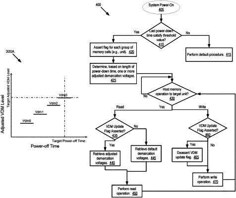
determining a length of time the memory device has been powered off; and
in response to determining that the length of time satisfies a threshold criterion:
for each group of a plurality of groups of memory cells, asserting a flag that corresponds to a respective group of the plurality of groups of memory cells;
determining, based on the length of time, an adjusted demarcation voltage to be used in reading a state of memory cells within each of the plurality of groups of memory cells; and
in response to receipt of a read operation directed to a group of memory cells of the plurality of groups of memory cells:
determining that a flag associated with the group of memory cells is asserted; and
performing the read operation using the adjusted demarcation voltage that was determined for the group of memory cells.
|