US 11,756,150 B2
Disaggregation of system-on-chip (SOC) architecture
Naveen Matam, Rancho Cordova, CA (US); Lance Cheney, El Dorado Hills, CA (US); Eric Finley, Ione, CA (US); Varghese George, Folsom, CA (US); Sanjeev Jahagirdar, Folsom, CA (US); Altug Koker, El Dorado Hills, CA (US); Josh Mastronarde, Sacramento, CA (US); Iqbal Rajwani, Roseville, CA (US); Lakshminarayanan Striramassarma, Folsom, CA (US); Melaku Teshome, El Dorado Hills, CA (US); Vikranth Vemulapalli, Folsom, CA (US); and Binoj Xavier, Folsom, CA (US)
Assigned to Intel Corporation, Santa Clara, CA (US)
Filed by Intel Corporation, Santa Clara, CA (US)
Filed on Feb. 17, 2022, as Appl. No. 17/674,781.
Application 17/674,781 is a continuation of application No. 17/500,375, filed on Oct. 13, 2021.
Application 17/500,375 is a continuation of application No. 17/069,188, filed on Oct. 13, 2020, granted, now 11,410,266.
Application 17/069,188 is a continuation of application No. 16/355,377, filed on Mar. 15, 2019, granted, now 10,803,548, issued on Oct. 13, 2020.
Prior Publication US 2022/0180468 A1, Jun. 9, 2022
Int. Cl. G06T 1/20 (2006.01); G06F 13/40 (2006.01)
CPC G06T 1/20 (2013.01) [G06F 13/4027 (2013.01)] 22 Claims
OG exemplary drawing
 
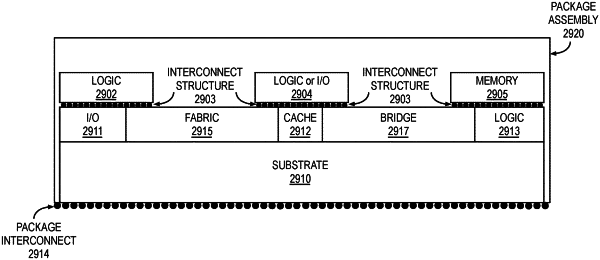
1. A multi-chip module comprising:
a plurality of semiconductor dies and a plurality of die-to-die interconnects, the plurality of semiconductor dies comprising:
a first semiconductor die including:
a plurality of graphics processing resources including a graphics multiprocessor, the graphics multiprocessor coupled with a first cache memory;
an interconnect fabric coupled with the first cache memory, wherein the first cache memory is associated with the graphics multiprocessor; and
a second cache memory coupled with the interconnect fabric, the interconnect fabric to couple the second cache memory with the first cache memory; and
a second semiconductor die coupled with the first semiconductor die in a 2.5-dimensional (2.5D) or 3-dimensional (3D) arrangement, the second semiconductor die including a third cache memory, wherein the third cache memory is accessible to the plurality of graphics processing resources of the first semiconductor die.