| CPC G06F 30/327 (2020.01) [G06F 2111/06 (2020.01); G06F 2119/18 (2020.01)] | 20 Claims |

|
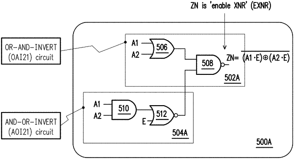
1. A logic circuit comprising:
first and second inverters; and
transistors configured such that:
first and second sets thereof represent corresponding first and second NAND circuits;
a third set thereof represents a transmission gate; and
a fourth set thereof represents a transmission-gate-substitute (TGS) circuit; and
wherein:
a first input of each of the first and second NAND circuits is configured to receive corresponding first and second data signals;
a second input of each of the first and second NAND circuits is configured to receive an enable signal;
the first inverter is configured to receive an output of the first NAND circuit;
the third and fourth sets are arranged as a combination circuit, representing one of an exclusive OR (XOR) circuit or an exclusive NOR (XNR) circuit, and being configured to receive:
an output of the second NAND circuit as a data input; and
an output of the first inverter and an output of the second NAND circuit as control inputs;
the second inverter is configured to receive an output of the combination circuit; and
an output of the second inverter represents one of an enable XOR (EXOR) function or an enable XNR (EXNR) function applied to the first and second data signals and the enable signal.
|