| CPC G06F 13/4022 (2013.01) [G06F 12/00 (2013.01); G06F 13/00 (2013.01); G06F 13/1673 (2013.01); G06F 13/1694 (2013.01)] | 17 Claims |
|
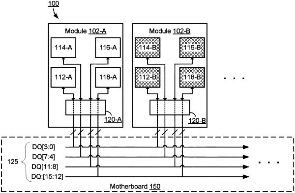
1. A memory controller for controlling a set of memory modules, the memory controller comprising:
a command/address interface to communicate commands and addresses to at least a first memory module and a second memory module;
a data interface including at least a first subset of memory controller data pins to communicate data with the first memory module and at least a second subset of memory controller data pins to communicate data with the second memory module;
a select interface to select between a first rank of memory devices and a second rank of memory devices,
wherein the first rank of memory devices includes at least one memory device of the first memory module coupled to the first subset of the memory controller data pins and at least one memory device of the second memory module coupled to the second subset of the memory controller data pins; and
wherein the second rank of memory devices including at least one memory device of the first memory module coupled to the first subset of the memory controller data pins and at least one memory device of the second memory module coupled to second subset of the memory controller data pins; and
configuration control logic to control a connectivity configuration of at least the first memory module by controlling which memory module data pins of the first memory module are enabled for communicating with the memory controller.
|