| CPC G06F 13/28 (2013.01) [G06F 3/0659 (2013.01); G06F 3/0661 (2013.01); G06F 12/10 (2013.01); G06F 12/1027 (2013.01); G06F 13/1668 (2013.01); H01L 23/5385 (2013.01); H01L 23/5386 (2013.01); G06F 2212/65 (2013.01); H01L 25/0652 (2013.01); H01L 25/0657 (2013.01); H01L 25/18 (2013.01); H01L 2225/0652 (2013.01); H01L 2225/06513 (2013.01); H01L 2225/06517 (2013.01); H01L 2225/06541 (2013.01); H01L 2225/06565 (2013.01); H01L 2225/06586 (2013.01); H01L 2924/1434 (2013.01); H01L 2924/15192 (2013.01); H01L 2924/15311 (2013.01)] | 20 Claims |
|
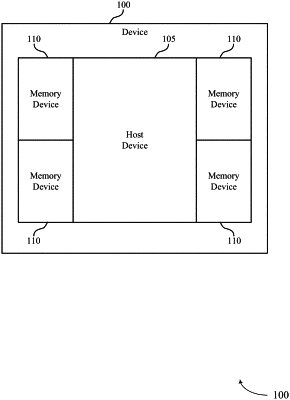
1. A system, comprising:
a host device configured to communicate with memory devices using a first communication protocol;
a memory device comprising logic for implementing at least a portion of operations associated with a memory controller of the memory device and being configured to communicate with the host device using a second communication protocol different than the first communication protocol;
a silicon interposer comprising a first area for the host device, a second area for memory devices configured to communicate with the host device using the first communication protocol, and a first plurality of channels between the first area and the second area, wherein the host device is positioned on the first area of the silicon interposer and the first plurality of channels support the first communication protocol; and
a translation device positioned on the second area of the silicon interposer, distinct from the logic for implementing at least the portion of operations associated with the memory controller, and configured to communicate with the host device via the first plurality of channels in the silicon interposer using the first communication protocol and with the memory device via a second plurality of channels in an organic substrate that is coupled with the translation device and the memory device using the second communication protocol.
|