| CPC G06F 12/0873 (2013.01) [G06F 9/4498 (2018.02); G06F 12/0246 (2013.01); G06F 12/0804 (2013.01); G06F 12/0862 (2013.01); G06F 13/1673 (2013.01); G06F 2212/7201 (2013.01)] | 20 Claims |
|
1. A system comprising:
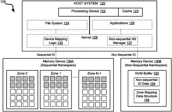
a plurality of integrated circuit (IC) dice having memory cells; and
a processing device coupled to the plurality of IC dice, the processing device to perform operations comprising:
causing a logic to enter an initial state associated with a first group of memory cells in response to an input-output (IO) write request directed at the first group of memory cells;
retrieving a write pointer that comprises a location within the first group of memory cells;
causing the logic to transition from the initial state to a sequential IO state; and
in response to determining the IO write request is directed to the location of the write pointer, causing data of the IO write request to be written to the plurality of IC dice starting at the location of the write pointer.
|