| CPC G06F 12/0253 (2013.01) [G06F 12/0246 (2013.01); G06F 12/0897 (2013.01); G06F 12/128 (2013.01)] | 20 Claims |
|
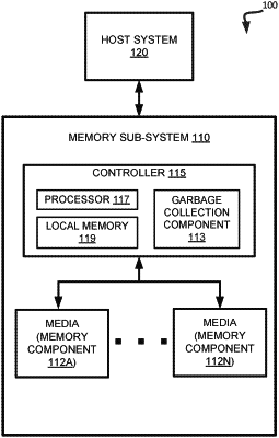
1. A method comprising:
initiating, by a processing device, a process to write valid data of at least a first block of a plurality of blocks stored at a first memory to a second memory, wherein the first memory has a first memory type and the second memory has a second memory type different from the first memory type;
identifying, by the processing device, at least one indicator relating to when data was written to the plurality of blocks stored at the first memory;
determining, by the processing device, whether an age of the valid data of the first block exceeds a threshold age based on the at least one indicator; and
in response to determining that the age of the valid data of the first block exceeds the threshold age, writing, by the processing device, the valid data of the first block to the second memory.
|