| CPC G06F 11/1072 (2013.01) [G11C 11/1675 (2013.01)] | 20 Claims |
|
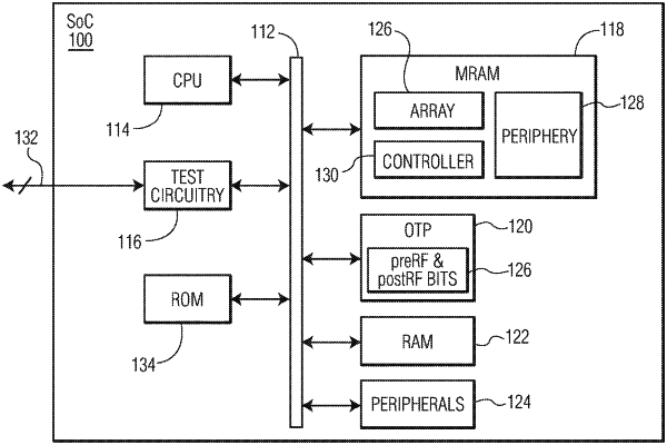
1. A method of programming a nonvolatile magnetoresistive random access memory (MRAM) device, the method comprising:
before a solder reflow process, combining separate words of MRAM data to form longer words of MRAM data;
assigning to each longer word a number of error correction code (ECC) bits in accordance with a first bit error correction rate that is less than a total number of error correction code (ECC) bits in accordance with a second bit error correction rate originally allocated to the respective separate words combined to form the longer word;
programming data into data bit cells of the MRAM as the longer words, wherein the programming includes, for each of the longer words:
inverting ones and zeros of each respective separate word when storing the respective separate word into the data bits cells as the longer word when the number of zeros is greater than the number of ones to be programmed in the data bit cells;
storing an inversion indicator bit for each respective separate word into the data bit cells to indicate whether the respective separate word has been inverted due to a number of zeros being greater than a number of ones to be programmed in the data bit cells; and
storing ECC bits generated from the longer word in accordance with the first bit error correction rate into the data bit cells.
|