| CPC G06F 7/5443 (2013.01) [G06N 3/04 (2013.01); G06N 3/065 (2023.01); H01L 29/7869 (2013.01)] | 10 Claims |
|
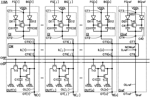
1. A semiconductor device comprising:
an offset circuit;
a first memory cell; and
a second memory cell,
wherein the offset circuit comprises a first constant current circuit, a second constant current circuit, first to third transistors, a first capacitor, a first wiring, a second wiring, a first output terminal, a second output terminal, and a current mirror circuit,
wherein the first constant current circuit comprises a fourth transistor, a first diode, and a second capacitor,
wherein the fourth transistor comprises a first gate and a second gate,
wherein the second constant current circuit comprises a fifth transistor, a second diode, and a third capacitor,
wherein the fifth transistor comprises a first gate and a second gate,
wherein a first terminal of the first transistor is electrically connected to a first terminal of the second transistor,
wherein a gate of the first transistor is electrically connected to a second terminal of the second transistor,
wherein the first terminal of the second transistor is electrically connected to the first wiring,
wherein a first terminal of the third transistor is electrically connected to the second terminal of the second transistor,
wherein a first terminal of the first capacitor is electrically connected to the gate of the first transistor,
wherein a first terminal of the fourth transistor is electrically connected to the first wiring,
wherein the first gate of the fourth transistor is electrically connected to a first terminal of the second capacitor,
wherein the second gate of the fourth transistor is electrically connected to the first terminal of the fourth transistor,
wherein a second terminal of the second capacitor is electrically connected to the first terminal of the fourth transistor,
wherein an output terminal of the first diode is electrically connected to the first gate of the fourth transistor,
wherein a first terminal of the fifth transistor is electrically connected to the second wiring,
wherein the first gate of the fifth transistor is electrically connected to a first terminal of the third capacitor,
wherein the second gate of the fifth transistor is electrically connected to the first terminal of the fifth transistor,
wherein a second terminal of the third capacitor is electrically connected to the first terminal of the fifth transistor,
wherein an output terminal of the second diode is electrically connected to the first gate of the fifth transistor,
wherein the first wiring is electrically connected to the first output terminal,
wherein the second wiring is electrically connected to the second output terminal,
wherein the current mirror circuit is configured to output a first current corresponding to a potential of the second wiring to each of the first wiring and the second wiring,
wherein the first memory cell is electrically connected to the first output terminal, and
wherein the second memory cell is electrically connected to the second output terminal.
|