| CPC G06F 1/3225 (2013.01) [G06F 1/14 (2013.01); G06F 1/3246 (2013.01); G06F 1/3253 (2013.01); G06F 1/3275 (2013.01); G11C 7/106 (2013.01); G11C 7/1087 (2013.01)] | 21 Claims |
|
1. A system comprising:
a memory device; and
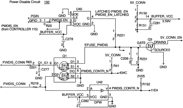
a power disable circuit coupled to a bus connector of a host system and to power circuitry adapted to power on and off the memory device, the power disable circuit comprising:
a first field effect transistor (FET) and a second FET with sources mutually coupled and gates to receive a power disable (PWDIS) signal of the bus connector, wherein, in response to an asserted input of the PWDIS signal at a second gate of the second FET, a drain of the first FET is left floating;
a latch circuit to assert an output in response to a general purpose input/output signal received from a processing device; and
a third FET coupled to the drain of the first FET and to the output of the latch circuit, wherein in response to assertion of the output of the latch circuit, the third FET is to signal to the power circuitry to cut power to the memory device.
|