| CPC G03F 7/0007 (2013.01) [G02B 6/122 (2013.01); G02B 6/136 (2013.01)] | 20 Claims |
|
1. A method of forming a plurality of slanted nanostructures using a lithography tool, comprising:
performing a first process comprising:
depositing a first layer comprising a first material on a first surface of a transparent substrate;
removing one or more first portions of the first layer comprising the first material to form one or more trenches; and
depositing a second layer comprising a second material in the one or more trenches to form a first alternating layer comprising alternating first remaining portions comprising the first material disposed in contact with second portions comprising the second material, the second material being different than the first material;
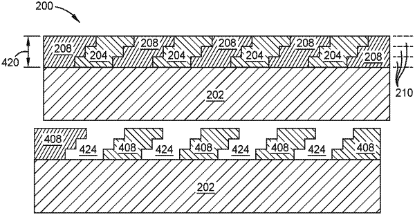
repeating the first process one or more times to form one or more additional alternating layers over the first alternating layer, each first remaining portion of each alternating layer in contact with and offset a first distance from an adjacent first remaining portion in adjacent alternating layers; and
performing a second process comprising:
removing each second portion from each alternating layer; and
etching sidewalls of each first remaining portion to smooth the sidewalls to form the plurality of slanted nanostructures comprising the first material, each of the plurality of slanted nanostructures disposed at an angle from 0° to about 90° from the first surface of the transparent substrate.
|
|
8. A method of forming a plurality of slanted nanostructures using a lithography tool, comprising:
performing a first process comprising:
depositing a first layer comprising a first material on a transparent substrate;
removing one or more first portions of the first layer comprising the first material to form one or more trenches;
depositing a second layer comprising a second material over the first material and in the one or more trenches, the second material being different than the first material; and
etching and planarizing the second layer comprising the second material to form a first alternating layer comprising first remaining portions comprising the first material disposed in contact with second remaining portions comprising the second material, the first alternating layer having a thickness from about 10 nm to about 100 μm;
repeating the first process one or more times to form one or more additional alternating layers over the first alternating layer, each second remaining portion of each alternating layer disposed in contact with and offset a first distance from an adjacent second remaining portion in adjacent alternating layers; and
performing a second process comprising:
removing each first remaining portion from each alternating layer; and
etching sidewalls of each second remaining portion to form the plurality of slanted nanostructures comprising the second material.
|
|
15. A method of forming a plurality of slanted nanostructures using a lithography tool, comprising:
performing a first process comprising:
depositing a first layer comprising a first material on a first surface of a transparent substrate, the first material comprising Ti, Sb, Sn, Zr, Al, or Hf;
removing one or more first portions of the first layer comprising the first material to form one or more trenches; and
depositing a second layer comprising a second material in the one or more trenches to form a first alternating layer comprising alternating first remaining portions comprising the first material disposed in contact with second portions comprising the second material, the second material comprising an organic planarization layer, spin on glass, SiN, or a Si containing material;
repeating the first process one or more times to form one or more additional alternating layers over the first alternating layer, each first remaining portion of each alternating layer disposed in contact with and offset a first distance from an adjacent first remaining portion in adjacent alternating layers, and wherein each first remaining portions has a first width, the first width being greater than the first distance; and
performing a second process comprising:
removing either each first remaining portion or each second portion from each alternating layer to form the plurality of slanted nanostructures; and
etching sidewalls of each of the plurality of slanted nanostructures to smooth the sidewalls.
|