| CPC G02F 1/136209 (2013.01) [G02F 1/1368 (2013.01); G02F 1/136286 (2013.01); H01L 27/1244 (2013.01); H01L 27/1255 (2013.01)] | 13 Claims |

|
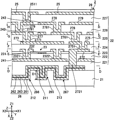
1. An electro-optical device including:
a substrate having a recessed portion that extends in a first direction;
a laminated film having a first conductive film, a dielectric film, and a second conductive film;
a first insulating film;
a light shielding film;
a second insulating film;
a semiconductor film including a source region, a channel region, and a drain region that are disposed in this order in the first direction; and
a drain electrode, wherein
the laminated film, the first insulating film, the light shielding film, the second insulating film, and the semiconductor film are disposed in this order from the substrate side, and the semiconductor film overlaps with the recessed portion and is disposed along the recessed portion as viewed in plan view,
the semiconductor film has a low concentration drain region between the drain region and the channel region, the low concentration drain region having a dopant concentration lower than a dopant concentration of the drain region,
a width of a bottom surface of the recessed portion along a second direction intersecting with the first direction is equal to or less than a width of the source region along the second direction,
the drain electrode overlaps with the low concentration drain region and the bottom surface as viewed in plan view,
as viewed in plan view, a contact hole for coupling the light shielding film and a gate electrode to each other is disposed on both sides of the low concentration drain region, and
as viewed in plan view, a contact hole for coupling a relay electrode that is coupled to the drain electrode and the first conductive film to each other is disposed on a side of the drain region opposite to the low concentration drain region.
|