| CPC G02F 1/133611 (2013.01) [G02F 1/133603 (2013.01); G02F 1/133607 (2021.01); G02F 1/133608 (2013.01)] | 9 Claims |
|
1. A backlight device comprising:
a substrate;
a plurality of light emitting elements disposed above the substrate; and
a diffuser plate having an incident surface disposed facing to the substrate, and an emitting surface disposed on an opposite side of the incident surface, diffusing light incident on the incident surface from the plurality of light emitting elements, and emitting the diffused light from the emitting surface;
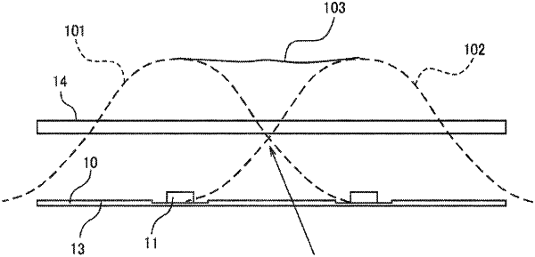
wherein a half value region is defined in which light that is equal to or more than half of a peak value of a brightness of light emitted from one of the plurality of light emitting elements is incident on the incident surface,
wherein the plurality of light emitting elements are disposed so that an overlapping ratio is 20% or less, and
wherein the overlapping ratio is a ratio of an area of an overlapping region to the area of the half value region defined around the one of the light emitting elements, and the overlapping region is a region overlapping the half value region defined around the one of the light emitting elements and a half value region defined around another one of the light emitting elements adjacent to the one of the light emitting elements.
|