| CPC G02B 6/12004 (2013.01) [G02B 6/13 (2013.01); H05K 1/0274 (2013.01); H05K 1/0298 (2013.01); H05K 3/007 (2013.01); H05K 3/0061 (2013.01); H05K 3/4611 (2013.01); H05K 2201/10106 (2013.01); H05K 2201/10121 (2013.01)] | 5 Claims |
|
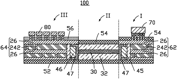
1. A photoelectric composite circuit board, comprising:
a first area comprising a first circuit substrate, a first coupling element, and a chip, both the first coupling element and the chip electrically connected to the first circuit substrate;
a second area connected to the first area, the second area comprising an optical fiber and an insulating layer, two opposite ends of the optical fiber being accommodated in the insulating layer; and
a third area disposed on a side of the second area away from the first area, the third area comprising a second circuit substrate, a second coupling element, and an electronic component, and both the second coupling element and the electronic component electrically connected to the second circuit substrate;
wherein the first coupling element is disposed at an end of the first circuit substrate adjacent to the second area; the second coupling element is disposed at an end of the second circuit substrate adjacent to the second area; both the first coupling element and the second coupling element are optically aligned with the optical fiber; both the first coupling element and the second coupling element are spaced apart from the optical fiber and are connected to the optical fiber through a transparent glue.
|