US 11,754,610 B2
Charge detection sensor and potential measurement system
Jun Ogi, Tokyo (JP); Yuri Kato, Kanagawa (JP); Naohiko Kimizuka, Kanagawa (JP); Yoshihisa Matoba, Kanagawa (JP); and Kan Shimizu, Kanagawa (JP)
Assigned to SONY SEMICONDUCTOR SOLUTIONS CORPORATION, Kanagawa (JP)
Appl. No. 16/646,185
Filed by SONY SEMICONDUCTOR SOLUTIONS CORPORATION, Kanagawa (JP)
PCT Filed Aug. 14, 2018, PCT No. PCT/JP2018/030255
§ 371(c)(1), (2) Date Mar. 11, 2020,
PCT Pub. No. WO2019/058815, PCT Pub. Date Mar. 28, 2019.
Claims priority of application No. 2017-179872 (JP), filed on Sep. 20, 2017.
Prior Publication US 2020/0271710 A1, Aug. 27, 2020
Int. Cl. G01R 29/24 (2006.01); G01N 27/414 (2006.01)
CPC G01R 29/24 (2013.01) [G01N 27/4145 (2013.01)] 13 Claims
OG exemplary drawing
 
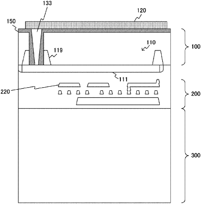
1. A charge detection sensor, comprising:
a detection element on a first surface of a semiconductor substrate, wherein the detection element is configured to detect a charge;
a detection electrode on a second surface of the semiconductor substrate, wherein
the first surface is different from the second surface; and
a contact that penetrates the semiconductor substrate, wherein
the contact is configured to electrically connect the detection electrode and the detection element, and
the contact is directly connected to a terminal of the detection element.