| CPC G01R 19/0084 (2013.01) [G01R 31/396 (2019.01); H01M 10/48 (2013.01); H01M 10/482 (2013.01)] | 15 Claims |
|
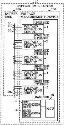
1. A voltage measurement device, comprising:
a plurality of voltage detection circuits which measure cell voltages of a plurality of cells connected in series from a lowermost side to an uppermost side,
wherein each of the plurality of voltage detection circuits includes a lowermost voltage detection circuit, an uppermost voltage detection circuit and one or more middle voltage detection circuits disposed between the lowermost voltage detection circuit and the uppermost voltage detection circuit, each of the one or more middle voltage detection circuits includes:
a device address generating circuit which generates a device address according to a first address assignment command received from a preceding voltage detection circuit located at a preceding stage; and
an address assignment command generating circuit which generates a second address assignment command according to the first address assignment command, and sends the second address assignment command to a next voltage detection circuit located at a next stage,
the preceding voltage detection circuit is one of a lower voltage detection circuit located at a lower side or an upper voltage detection circuit located at an upper side among the plurality of voltage detection circuits, and the next voltage detection circuit is the other of the lower voltage detection circuit or the upper voltage detection circuit among the plurality of voltage detection circuits, and
the device address generating circuit generates a same device address for (i) the device address according to the first address assignment command received from the lower voltage detection circuit and (ii) the device address according to the first address assignment command received from the upper voltage detection circuit.
|