| CPC G01N 21/9501 (2013.01) [G01N 21/8806 (2013.01); G01N 21/956 (2013.01); H01L 22/12 (2013.01)] | 16 Claims |
|
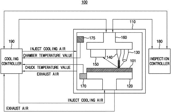
1. A semiconductor wafer inspection system comprising:
a wafer chuck disposed inside a chamber and on which a wafer is disposed;
a light source configured to emit light to the wafer so as to inspect a pattern on the wafer;
an inspection controller configured to control driving of the light source;
a cooling gas gun disposed adjacent to the light source and configured to spray a cooling gas on a surface of the wafer;
a temperature sensor configured to measure a temperature of the wafer chuck, generate a temperature value, and transmit the temperature value to a cooling controller; and
the cooling controller comprising:
a first cooler configured to generate and supply cooling air to the wafer chuck before light is emitted to the wafer;
a second cooler configured to generate and supply the cooling gas to the cooling gas gun; and
a driving controller configured to control driving of the first cooler based on the temperature of the wafer chuck and control driving of the second cooler based on a point in time at which light is emitted to the wafer.
|