| CPC C30B 29/04 (2013.01) [C23C 16/0281 (2013.01); C23C 16/277 (2013.01); C23C 16/279 (2013.01); C30B 25/18 (2013.01); C30B 25/183 (2013.01); C30B 25/20 (2013.01); H01F 1/40 (2013.01); C01B 32/25 (2017.08); H01F 10/10 (2013.01); Y10T 428/30 (2015.01)] | 4 Claims |
|
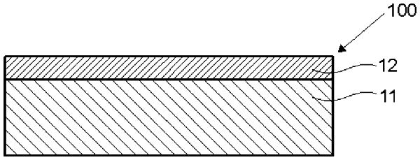
1. A diamond substrate comprising a diamond crystal layer having nitrogen-vacancy centers and no silicon-vacancy centers, wherein a light intensity INV− of an NV− center light (wavelength: 637 nm) is INV−≥2800 counts when the diamond crystal layer having the nitrogen-vacancy centers and no silicon-vacancy centers is measured by a photoluminescence apparatus under conditions:
an excitation light wavelength of 532 nm;
an excitation light intensity of 2.0 mW;
a total time of 1 second; a total number of 3 times;
a hole diameter of 100 μm;
an objective lens with a magnification of 15; and
measurement in room temperature of 298 K.
|