| CPC C25D 7/12 (2013.01) [C23C 14/18 (2013.01); C25D 3/54 (2013.01)] | 11 Claims |

|
1. A method of fabricating a wafer stack, the method comprising:
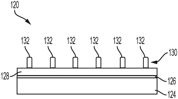
forming a tantalum-nitride film on a substrate of the wafer stack using physical vapor deposition in a deposition chamber of a physical vapor deposition apparatus controlled by a deposition controller;
forming a tantalum layer on the tantalum-nitride film using physical vapor deposition in the deposition chamber controlled by the deposition controller, wherein the tantalum layer is at least three times thicker than the tantalum-nitride film, and an average sheet resistance of the tantalum layer and the tantalum-nitride film combined on the substrate is between 0.1 and 1.0 ohms-per-square; and
depositing indium directly on the tantalum layer using electroplating in an electroplating bath of an electroplating apparatus controlled by an electroplating controller.
|