| CPC C23C 16/45534 (2013.01) [C23C 16/402 (2013.01); C23C 16/45527 (2013.01)] | 5 Claims |
|
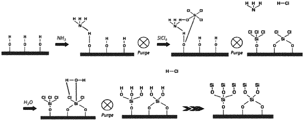
1. A method for atomic layer deposition for a coating of silicon oxide on a substrate, such as on an inorganic material, and performed at room temperature, involving at least three precursors, the at least three precursors being silicon tetrachloride, water and one Lewis base agent, said method comprising the sequential and non-overlapping steps of:
a) exposing the one Lewis base agent to the substrate during a first exposure time;
b) exposing the silicon tetrachloride to the substrate during a second exposure time; and
c) exposing the water to the substrate during a third exposure time,
wherein a step of purging with nitrogen gas is performed after step (a), and at least one step of purging with nitrogen gas is performed after each of the steps (b) and (c) for obtaining a porous silicon dioxide film onto the substrate, wherein the level of chlorine contaminants is less than 3% of the total mass of the silicon dioxide film, and
wherein each of the steps (a), (b) and (c) is performed at room temperature.
|