| CPC C23C 16/4405 (2013.01) [B08B 3/08 (2013.01); B08B 7/005 (2013.01); B08B 7/0042 (2013.01); C23C 16/4407 (2013.01); C23C 16/45565 (2013.01)] | 20 Claims |
|
1. A method for cleaning a semiconductor fabrication equipment part used for processing semiconductor wafers,
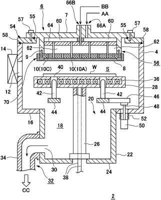
wherein the semiconductor fabrication equipment part comprises a distribution plate formed of aluminum or aluminum alloy and having a plurality of gas holes,
the method comprising:
step (1): scanning a gas injection surface of the distribution plate, which is a surface facing the wafer, with a laser beam to remove deposits adhered to a surface of the gas injection surface and deposits near a surface of at least one of the plurality of gas holes, and to crack a film of the deposits adhered to inside of said at least one of the plurality of gas holes, or to peel a film of the deposits from the inside of said at least one of the plurality of gas holes, wherein the laser beam is infrared and an average energy density of the laser beam is 1×10³ to 1×10¹¹ W/m2; and
step (2): bringing the gas injection surface and the inside of said at least one of the plurality of gas holes into contact with a cleaning liquid containing an inorganic acid, and allowing the cleaning liquid to penetrate cracks in the film of the deposits or gaps between the film of the deposits and the inside of said at least one of the plurality of gas holes to clean the semiconductor fabrication equipment part having the plurality of gas holes.
|