| CPC B81C 1/00349 (2013.01) [B81C 1/00325 (2013.01); B81C 3/001 (2013.01)] | 15 Claims |
|
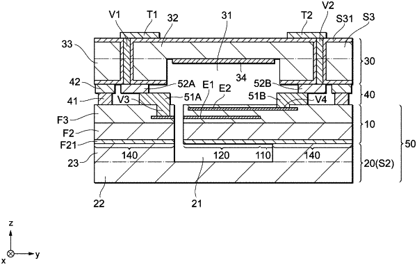
1. A MEMS device comprising:
a lower substrate having a resonator that includes a lower electrode, an upper electrode, and a piezoelectric film disposed therebetween;
an upper substrate that opposes the resonator;
a bonding layer that seals an internal space between the lower substrate and the upper substrate; and
a wiring layer that contains a same metal material as the bonding layer,
wherein the wiring layer comprises a rare gas content that is less than 1×10²⁰ (atoms/cm3),
wherein the wiring layer is disposed in the internal space and not directly coupled to the bonding layer,
wherein the wiring layer comprises a pair of wiring layers that electrically couples an external terminal to one of the lower electrode and the upper electrode of the resonator,
wherein a first wiring layer of the pair of wiring layers is offset in a thickness direction relative to a second wiring layer of the pair of wiring layers, such that a non-eutectic portion is provided in a region away from a contact area between the first and second wiring layers, and
wherein the thickness direction is measured in a directional normal to a surface of the piezoelectric film.
|