| CPC B32B 17/10504 (2013.01) [B32B 3/04 (2013.01); B32B 17/10036 (2013.01); B32B 17/10761 (2013.01); B32B 37/182 (2013.01); B32B 38/10 (2013.01); B32B 2305/55 (2013.01); B32B 2307/71 (2013.01); B32B 2605/08 (2013.01)] | 20 Claims |
|
1. A functional element having electrically controllable optical properties, comprising:
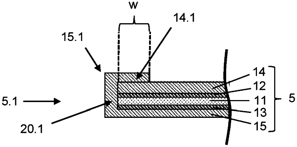
a stack sequence consisting of, successively along a thickness of the stack sequence, a first carrier film, a first surface electrode, with the first surface electrode being arranged on an inward surface of the first carrier film and bonded directly thereto, an active layer, a second surface electrode, and a second carrier film, with the second surface electrode being arranged between the active layer and the second carrier film and on an inward surface of the second carrier film and bonded directly thereto, the active layer being between the first and second surface electrodes and in direct contact with the first and second surface electrodes, wherein the second carrier film consists of a single film made with a same material composition, wherein
the second carrier film is folded around the first carrier film at least at one side edge and seals an exit surface of the active layer at the side edge,
at least one section of an overhanging region of the second carrier film is materially bonded to an edge region of the first carrier film, by permanently pressing the at least one section and the edge region together, by fusing the at least one section to the edge region, and/or by gluing the at least one section to the edge region, and
the second carrier film is implemented such that the second carrier film prevents diffusion of plasticizers through the carrier film.
|