| CPC B29D 11/00403 (2013.01) [G02F 1/29 (2013.01); B29K 2995/0026 (2013.01); G02C 7/083 (2013.01); G02F 1/294 (2021.01)] | 16 Claims |
|
1. A holding system for supporting a wafer and an optical element, the wafer and the optical element being conformed to form an optical system, the wafer having a first surface adapted to a prescription of a wearer, a second surface opposed to the first surface, and a third surface joining the first surface and the second surface, the optical element having a first surface, a second surface opposed to the first surface, and a third surface joining the first surface and the second surface, the holding system comprising:
a support and positioning system configured to position the second surface of the wafer relative to the first surface of the optical element, the support and positioning system comprising
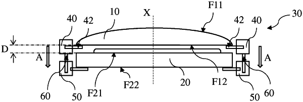
a first support configured to support at least part of one or more of: (i) the second surface and (ii) the third surface of the wafer, the first support comprising a plurality of blades, each of the blades being configured to support at least part of one or more of: (i) the second surface and (ii) the third surface of the wafer, and
a second support configured to support at least part of one or more of: (i) the second surface and (ii) the third surface of the optical element;
a mechanical system configured to move the first support and the second support one relative to the other to move the second surface of the wafer and the first surface of the optical element to form the optical system; and
a real-time measuring device configured to measure in real-time the distance between the second surface of the wafer and the second surface of the optical element,
wherein the mechanical system is configured to move each of the blades independently from each other based on the measured distance.
|