| CPC B23B 27/148 (2013.01) [B23B 2226/125 (2013.01)] | 20 Claims |
|
1. A cubic boron nitride sintered material comprising: cubic boron nitride particles in an amount of 70 vol % or more and less than 100 vol %, and a bonding material, wherein
the bonding material comprises an aluminum compound, and comprises cobalt as a constituent element;
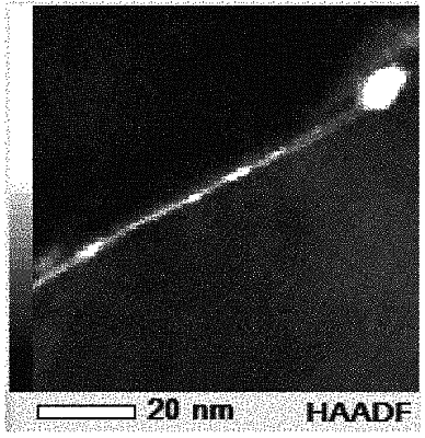
the cubic boron nitride sintered material has a first region in which a space between adjacent cubic boron nitride particles is 0.1 nm or more and 10 nm or less;
when the first region is analyzed by using an energy dispersive X-ray analyzer equipped with a transmission electron microscope, an atom % of aluminum in the first region is 0.1 or more; and
the first region is observed in 6 or more among 10 images of 100 nm×100 nm in size that are generated by imaging, at a magnification of 2,000,000×, a region in which a structure like an interface of the adjacent cubic boron nitride particles is formed in the cubic boron nitride sintered material.
|