| CPC A61B 8/4483 (2013.01) [B06B 1/0644 (2013.01); H10N 30/073 (2023.02); H10N 30/088 (2023.02); H10N 30/10516 (2023.02)] | 18 Claims |

|
1. A method, comprising:
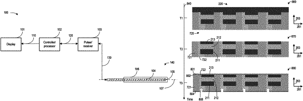
laminating a first comb structure and a second comb structure into an acoustic stack, the first comb structure having fins including a piezoelectric layer intermediate a matching layer and a backing layer, the second comb structure having fins and kerfs;
plating a first conductive layer over a top surface of the acoustic stack;
plating a second conductive layer over a bottom surface of the acoustic stack;
cutting a groove through the second conductive layer;
dicing the cut acoustic stack into an ultrasound transducer having a back face including a signal pad and a ground pad formed by the second conductive layer and separated by the groove; and
inserting a distal end of a flex attachment into the groove, the flex attachment having a proximal end configured to electrically couple to a processor, wherein the flex attachment includes a non-conductive middle layer intermediate a first conductive layer and a second conductive layer.
|