US 11,751,492 B2
Embedded memory pillar
Dexin Kong, Redmond, WA (US); Ashim Dutta, Clifton Park, NY (US); Ekmini Anuja De Silva, Slingerlands, NY (US); and Daniel Schmidt, Niskayuna, NY (US)
Assigned to INTERNATIONAL BUSINESS MACHINES CORPORATION, Armonk, NY (US)
Filed by INTERNATIONAL BUSINESS MACHINES CORPORATION, Armonk, NY (US)
Filed on Sep. 24, 2021, as Appl. No. 17/484,649.
Prior Publication US 2023/0099303 A1, Mar. 30, 2023
Int. Cl. G11C 13/00 (2006.01); H10N 70/00 (2023.01); H10B 61/00 (2023.01); H10B 63/00 (2023.01); H10N 50/01 (2023.01); H10N 50/10 (2023.01); H10N 50/80 (2023.01); H10N 50/85 (2023.01)
CPC H10N 70/068 (2023.02) [H10B 61/00 (2023.02); H10B 63/80 (2023.02); H10N 50/01 (2023.02); H10N 50/10 (2023.02); H10N 50/80 (2023.02); H10N 50/85 (2023.02); H10N 70/023 (2023.02); H10N 70/063 (2023.02); H10N 70/066 (2023.02); H10N 70/841 (2023.02)] 20 Claims
OG exemplary drawing
 
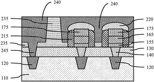
1. A memory device, comprising:
a memory stack on a first dielectric layer;
a sidewall spacer on the memory stack;
a conductive cap on the sidewall spacer and the memory stack; and
an upper metal line on the conductive cap and the sidewall spacer, wherein the upper metal line wraps around the conductive cap, sidewall spacer, and memory stack.