US 11,751,485 B2
Flat bottom electrode via (BEVA) top surface for memory
Hsia-Wei Chen, Taipei (TW); Chih-Yang Chang, Yuanlin Township (TW); Chin-Chieh Yang, New Taipei (TW); Jen-Sheng Yang, Keelung (TW); Sheng-Hung Shih, Hsinchu (TW); Tung-Sheng Hsiao, New Taipei (TW); Wen-Ting Chu, Kaohsiung (TW); Yu-Wen Liao, New Taipei (TW); and I-Ching Chen, Hsinchu (TW)
Assigned to Taiwan Semiconductor Manufacturing Company, Ltd., Hsinchu (TW)
Filed by Taiwan Semiconductor Manufacturing Company, Ltd., Hsin-Chu (TW)
Filed on Nov. 30, 2021, as Appl. No. 17/537,830.
Application 16/552,169 is a division of application No. 15/823,012, filed on Nov. 27, 2017, granted, now 10,566,519, issued on Feb. 18, 2020.
Application 17/537,830 is a continuation of application No. 16/939,583, filed on Jul. 27, 2020, granted, now 11,201,281.
Application 16/939,583 is a continuation of application No. 16/552,169, filed on Aug. 27, 2019, granted, now 10,763,426, issued on Sep. 1, 2020.
Claims priority of provisional application 62/547,230, filed on Aug. 18, 2017.
Prior Publication US 2022/0093849 A1, Mar. 24, 2022
Int. Cl. H10N 50/80 (2023.01); H01L 23/538 (2006.01); H01L 21/768 (2006.01); H10B 61/00 (2023.01); H10B 63/00 (2023.01); H10N 50/01 (2023.01); H10N 50/10 (2023.01); H10N 70/00 (2023.01); H10N 70/20 (2023.01)
CPC H10N 50/80 (2023.02) [H01L 21/768 (2013.01); H01L 23/5384 (2013.01); H10B 61/22 (2023.02); H10B 63/30 (2023.02); H10N 50/01 (2023.02); H10N 50/10 (2023.02); H10N 70/011 (2023.02); H10N 70/20 (2023.02); H10N 70/841 (2023.02); H10N 70/8833 (2023.02)] 20 Claims
OG exemplary drawing
 
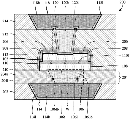
1. An integrated circuit (IC) comprising:
a first conductive feature;
a memory cell overlying the first conductive feature; and
a second conductive feature extending from the memory cell to the first conductive feature and comprising a lower conductive body, an upper conductive body, and a conductive liner, wherein the upper conductive body fully covers the lower conductive body when viewed in profile, wherein the conductive liner extends along a bottom surface of the lower conductive body and individual sidewalls of the lower and upper conductive bodies, and wherein a top surface of the lower conductive body and a bottom surface of upper conductive body directly contact each other.