| CPC H10K 59/88 (2023.02) [G09G 3/006 (2013.01); H01L 27/0292 (2013.01); H10K 59/131 (2023.02); G09G 2330/04 (2013.01); G09G 2330/12 (2013.01); H01L 27/0296 (2013.01); H02H 9/045 (2013.01)] | 20 Claims |
|
1. A display substrate, comprising:
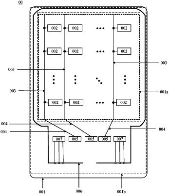
a base substrate comprising a display region and a peripheral region surrounding the display region;
a plurality of sub-pixels disposed in the display region; a plurality of data lines disposed in the display region and electrically connected to the plurality of sub-pixels;
a plurality of data transmission lines disposed in the peripheral region and electrically connected to the plurality of data lines;
a plurality of electrostatic discharge circuits disposed in the peripheral region and electrically connected to the plurality of data transmission lines, wherein the plurality of electrostatic discharge circuits are arranged along an extension direction of a boundary of the display region;
a panel crack detection trace disposed in the peripheral region and surrounding the display region; and
a plurality of electrostatic discharge dummy circuits disposed in the peripheral region and arranged along the extension direction of the boundary of the display region, wherein the plurality of electrostatic discharge dummy circuits are disposed on at least one side of the plurality of electrostatic discharge circuits along the extension direction of the boundary of the display region, and at least one of the plurality of electrostatic discharge dummy circuits is electrically connected to the panel crack detection trace and configured to discharge static electricity on the panel crack detection trace,
wherein the plurality of electrostatic discharge dummy circuits includes a first electrostatic protection line for discharging static electricity and the plurality of electrostatic discharge circuits includes a second electrostatic protection line for discharging static electricity, and the first electrostatic protection line and the second electrostatic protection line are shared.
|