| CPC H10K 59/40 (2023.02) [G06F 1/184 (2013.01); H10K 50/865 (2023.02); H10K 71/00 (2023.02); H10K 59/1201 (2023.02)] | 17 Claims |
|
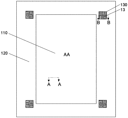
1. A display motherboard, comprising:
a display area and a peripheral area surrounding the display area, wherein the peripheral area comprises an alignment mark area;
an array substrate;
an alignment mark disposed on the array substrate and in the alignment mark area; and
a color film layer comprising a filter layer and a black matrix, wherein at least a portion of the black matrix is located in the alignment mark area,
wherein the portion of the black matrix in the alignment mark area comprises a first light-shielding portion and a second light-shielding portion, the first light-shielding portion covers the alignment mark, and the second light-shielding portion covers an area outside the alignment mark in the alignment mark area,
wherein a surface of the first light-shielding portion distal to the array substrate and a surface of the second light-shielding portion distal to the array substrate are not in a same plane, and
wherein the display motherboard further comprises:
an organic layer disposed on the array substrate and at least in the alignment mark area, wherein the organic layer has a hollow portion penetrating the array substrate in a thickness direction, the portion of the black matrix in the alignment mark area is disposed on one side of the organic layer distal to the array substrate, and the alignment mark is formed in the organic layer.
|