| CPC H10K 59/131 (2023.02) [H10K 71/00 (2023.02); H10K 59/1201 (2023.02); H10K 2102/341 (2023.02)] | 12 Claims |
|
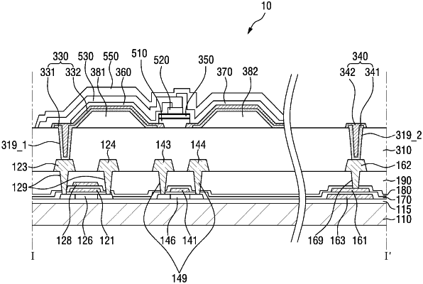
1. A display device comprising:
a substrate including a plurality of first pixels and a plurality of second pixels adjacent to the plurality of first pixels;
a plurality of pixel electrodes disposed on the substrate;
a plurality of common electrodes disposed on the substrate and spaced apart from the pixel electrodes;
a first insulating layer disposed on the substrate, and at least a portion of the first insulating layer disposed on each of the pixel electrode and the common electrode; and
a plurality of light emitting elements disposed on the first insulating layer, and at least portion of the light emitting elements overlapping the pixel electrode and the common electrode,
wherein the pixel electrode, the common electrode, and the light emitting element are disposed in each of the first pixel and the second pixel,
the common electrode of the first pixel and the common electrode of the second pixel are disposed adjacent to each other, and disposed between a first pixel electrode of the first pixel and a second pixel electrode of the second pixel.
|