| CPC H10K 59/131 (2023.02) [G09G 3/3233 (2013.01); G09G 2300/0426 (2013.01); G09G 2300/0819 (2013.01); G09G 2300/0842 (2013.01); G09G 2300/0861 (2013.01); G09G 2310/08 (2013.01); H10K 59/126 (2023.02)] | 13 Claims |
|
1. A display panel, comprising:
a base substrate; and
a plurality of sub-pixels located on the base substrate;
wherein each of the plurality of sub-pixels comprises:
a semiconductor layer located on the base substrate and comprising:
a first active layer of an initialization transistor,
a second active layer of a reset transistor, and
a third active layer of a data writing transistor;
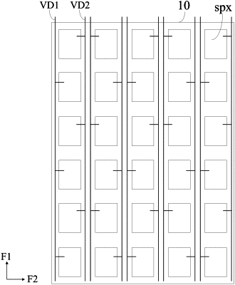
a first conductive layer located on a side, facing away from the base substrate, of the semiconductor layer and comprising: a data signal line extending in a first direction; and
a second conductive layer located on the base substrate and comprising: a drive gate of a drive transistor;
wherein the drive gate is electrically connected to a first conductive region of the first active layer;
the data signal line is electrically connected to a first conductive region of the third active layer; and
an orthographic projection of the second active layer on the base substrate is located between an orthographic projection of the first active layer on the base substrate and an orthographic projection of the data signal line on the base substrate.
|