| CPC H10K 59/131 (2023.02) [G06F 1/189 (2013.01); G09G 3/3208 (2013.01)] | 23 Claims |
|
1. A display device comprising a substrate comprising:
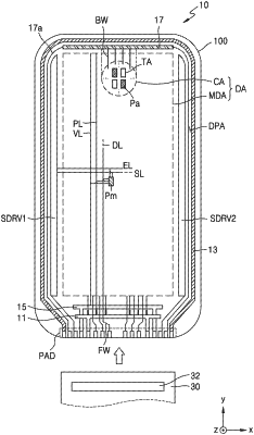
a main display area, main display elements being in the main display area;
a component area, auxiliary display elements and a transmission area being in the component area; and
a peripheral area outside the main display area;
an initialization voltage line in the main display area and extending in a first direction;
a bottom metal layer in the component area between the substrate and the auxiliary display elements; and
a bias line in the main display area and extending in the first direction,
the bias line being connected to the bottom metal layer and being at a same layer as the initialization voltage line,
wherein the bias line and the initialization voltage line are alternately arranged along a second direction crossing the first direction, in a first region of the main display area around the component area.
|