| CPC H10K 59/131 (2023.02) [H10K 50/844 (2023.02); H10K 50/8426 (2023.02); H10K 59/122 (2023.02); H10K 2102/311 (2023.02)] | 3 Claims |
|
1. A display device comprising:
a first display region and a second display region each including a plurality of optical elements, each of the plurality of optical elements including:
a first electrode provided for each pixel;
a second electrode provided in common to a plurality of pixels; and
a function layer sandwiched between the first electrode and the second electrode;
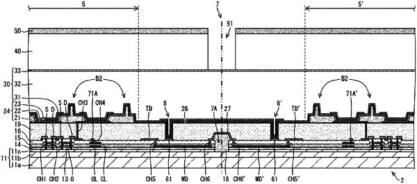
a curved portion provided between the first display region and the second display region;
a frame region surrounding the first display region, the second display region, and the curved portion;
a terminal portion provided with a terminal of a wiring line;
a bending portion provided between the frame region and the terminal portion;
a plurality of pixel circuits corresponding to the plurality of optical elements in each of the first and second display regions;
a plurality of first high power supply voltage lines configured to input a high power supply voltage to the plurality of pixel circuits in the first display region;
a plurality of second high power supply voltage lines configured to input a high power supply voltage to the plurality of pixel circuits in the second display region;
a first high power supply voltage trunk wiring line provided between the first display region and the second display region; and
a second high power supply voltage trunk wiring line provided between the first display region and the second display region,
wherein the plurality of first high power supply voltage lines branches from the first high power supply voltage trunk wiring line and extends to the first display region,
the plurality of second high power supply voltage lines branches from the second high power supply voltage trunk wiring line and extends to the second display region,
the first high power supply voltage trunk wiring line and the second high power supply voltage trunk wiring line are electrically connected to each other via a first curved portion conductive layer formed in the curved portion,
an opening is formed in at least one inorganic film forming a thin film transistor (TFT) layer in the curved portion,
a filling film is formed to fill the opening,
the first curved portion conductive layer is formed on the filling film,
a flattening film forming the TFT layer is provided with a first trench and a second trench to surround the first display region and the second display region, and
in the first trench and the second trench, the second electrode is in contact with an intermediate conductive film formed of the same material in the same layer as the first electrode.
|