| CPC H10K 59/131 (2023.02) [G09G 3/3225 (2013.01); H10K 59/1213 (2023.02); H10K 59/1216 (2023.02); G09G 2300/0426 (2013.01); G09G 2300/08 (2013.01); G09G 2320/0209 (2013.01); H01L 27/1214 (2013.01)] | 15 Claims |
|
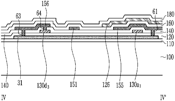
1. An organic light emitting diode display comprising:
a substrate;
a bridge electrode disposed on the substrate;
a buffer layer disposed on the bridge electrode;
a semiconductor layer disposed on the buffer layer;
a first gate insulating layer disposed on the semiconductor layer;
a first gate conductor disposed on the first gate insulating layer and which includes a first gate electrode;
a second gate insulating layer disposed on the first gate conductor;
a second gate conductor disposed on the second gate insulating layer;
an interlayer-insulating layer disposed on the second gate conductor; and
a data line disposed on the interlayer-insulating layer,
wherein the first gate electrode is directly connected to the bridge electrode through a fourth contact hole, the fourth contact hole is formed in the buffer layer and the first gate insulating layer and overlaps a portion of the first gate electrode disposed on the first gate insulating layer, the first gate electrode does not penetrate the second gate insulating layer,
the semiconductor layer is electrically connected to the bridge electrode, and
a capacitance exists between the data line and the bridge electrode.
|