| CPC H10K 59/131 (2023.02) [G09G 3/3266 (2013.01); G09G 3/3275 (2013.01); H10K 59/124 (2023.02); H10K 59/1213 (2023.02); H10K 77/111 (2023.02); H01L 27/124 (2013.01); H01L 27/1218 (2013.01); H01L 27/1248 (2013.01); H01L 27/1288 (2013.01); H10K 59/1201 (2023.02); H10K 2102/311 (2023.02)] | 14 Claims |
|
1. A display panel, comprising:
a display area and a base substrate;
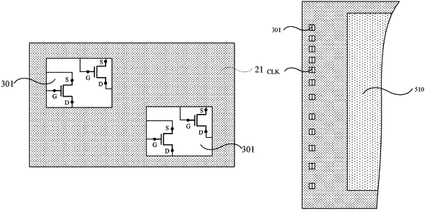
a driving circuit disposed in a periphery of the display area, and comprising a plurality of transistors;
at least one signal line on the base substrate; and
at least one insulating layer between the driving circuit and the at least one signal line, wherein an orthogonal projection of the at least one signal line on the base substrate has an overlapping area with an orthogonal projection of the driving circuit on the base substrate;
wherein the at least one signal line is at least one electrode power supply line, and the at least one electrode power supply line comprises at least one opening, and an area of an orthogonal projection of each opening of the at least one opening on the base substrate, is larger than an area of an orthogonal projection of a group of transistors among the plurality of transistors on the base substrate, the group of transistors comprises at least two transistors.
|