| CPC H10K 59/126 (2023.02) [G09G 3/3225 (2013.01); H10K 71/00 (2023.02); G09G 2300/0426 (2013.01); G09G 2300/0842 (2013.01); G09G 2320/0252 (2013.01); H10K 59/1201 (2023.02); H10K 59/131 (2023.02)] | 19 Claims |
|
1. A display panel, comprising:
a base substrate;
a light shielding layer disposed on the base substrate and comprising a plurality of light shielding patterns arranged in an array;
a buffer layer disposed on the base substrate and covering the light shielding layer;
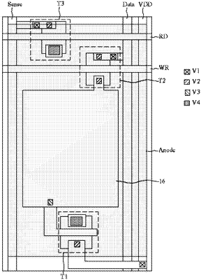
a thin-film transistor array layer comprising a plurality of thin-film transistors, wherein each of the thin-film transistors comprises an active layer, a gate line layer, a source electrode, and a drain electrode;
a display device layer disposed on a side of the thin-film transistor array layer away from the base substrate, and comprising an anode, a light-emitting layer, and a cathode disposed in a stack arrangement;
a plurality of first electrodes disposed on the same layer as the source electrode, wherein an orthographic projection area of each first electrode projected on the base substrate overlaps an orthographic projection area of the anode projected on the base substrate;
a storage capacitor comprising the first electrode and the anode; and
a plurality of signal lines arranged on a same layer as the light shielding patterns, wherein an orthographic projection area of at least one of the plurality of signal lines projected on the base substrate overlaps with the orthographic projection area of the anode.
|
|
13. A display panel, comprising:
a base substrate;
a light shielding layer disposed on the base substrate and comprising a plurality of light shielding patterns arranged in an array;
a buffer layer disposed on the base substrate and covering the light shielding layer;
a thin-film transistor array layer comprising a gate insulating layer, an interlayer dielectric layer, and a plurality of thin-film transistors, wherein each of the thin-film transistors comprises an active layer, a gate line layer, a source electrode, and a drain electrode, and the gate line layer is disposed on a side of the gate insulating layer away from the base substrate;
a display device layer disposed on a side of the thin-film transistor array layer away from the base substrate, and comprising an anode, a light-emitting layer, and a cathode disposed in a stack arrangement;
a plurality of first electrodes disposed on a same layer as the source electrode, wherein an orthographic projection area of each first electrode projected on the base substrate overlaps an orthographic projection area of the anode projected on the base substrate;
a storage capacitor comprising the first electrode and the anode; and
a plurality of signal lines arranged on a same layer as the light shielding patterns, wherein the plurality of signal lines comprise a data signal line, an orthographic projection area of the data signal line projected on the base substrate overlaps with the orthographic projection area of the anode, and the thin-film transistors are connected to the signal lines through via holes went through in the interlayer dielectric layer and the buffer layer.
|
|
17. A method of manufacturing a display panel, comprising:
providing a base substrate;
depositing a light shielding metal material on the base substrate, and etching the light shielding metal material to form a plurality of light shielding patterns and a plurality of signal lines at intervals;
forming a buffer layer on the base substrate, wherein the buffer layer covers the light shielding patterns;
depositing an active layer, a gate insulating layer, and a gate line layer sequentially on a side of the buffer layer away from the base substrate;
forming an interlayer dielectric layer on the side of the buffer layer away from the base substrate, wherein the interlayer dielectric layer covers the gate line layer, the gate insulating layer, and the active layer;
depositing a source/drain electrode material on the interlayer dielectric layer and etching the source/drain electrode material to form a source electrode, a drain electrode, and a first electrode;
forming a passivation protection layer on a side of the interlayer dielectric layer away from the buffer layer; and
forming an anode, a light-emitting layer, and a cathode sequentially on the passivation protection layer;
wherein an orthographic projection area of the anode projected on the base substrate overlaps an orthographic projection area of the first electrode projected on the base substrate; a storage capacitor comprising the anode and the first electrode, and the orthographic projection area of the anode overlaps with an orthographic projection area of at least one of the plurality of signal lines projected on the base substrate.
|