| CPC H10K 59/124 (2023.02) [H10K 59/126 (2023.02); H10K 59/1213 (2023.02); H10K 59/131 (2023.02); H10K 71/00 (2023.02); H01L 27/124 (2013.01); H01L 27/1225 (2013.01); H01L 27/1248 (2013.01); H01L 29/7869 (2013.01); H01L 29/78633 (2013.01); H10K 59/1201 (2023.02)] | 14 Claims |
|
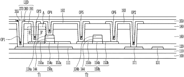
1. A display device comprising:
a substrate;
a first semiconductor layer disposed on the substrate, wherein the first semiconductor layer includes a channel region and a doped region;
a first gate electrode disposed to overlap the channel region of the first semiconductor layer;
an intermediate film disposed on the first semiconductor layer and the first gate electrode;
a first electrode disposed on the intermediate film; and
an light emitting layer disposed on the first electrode,
wherein an opening is defined through the intermediate film to overlap the doped region of the first semiconductor layer,
the doped region of the first semiconductor layer and the first electrode contact each other through the opening of the intermediate film,
an area of a cross-section of the opening of the intermediate film parallel to the substrate is in a range of about 49 μm2 to about 81 μm2, and
the light emitting layer directly contacts the first electrode.
|