| CPC H10K 59/122 (2023.02) [H10K 50/818 (2023.02); H10K 50/844 (2023.02); H10K 59/353 (2023.02)] | 20 Claims |
|
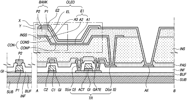
1. An organic light emitting display panel comprising:
a substrate including an active area having a plurality of subpixels, an image displayed in the active area;
an insulating film over the substrate, the insulating film including a concave portion in the active area of a subpixel from the plurality of subpixels, the concave portion having a flat portion, an inclined portion that extends from the flat portion, and a side portion that extends from the inclined portion, the side portion farther from the substrate than the inclined portion and the flat portion;
a first electrode disposed on the flat portion, the inclined portion, and the side portion of the concave portion of the insulating film;
a bank on the first electrode, the bank including a first part and a second part, wherein the first part of the bank overlaps the inclined portion of the insulating film and the second part of the bank overlaps the side portion of the insulating film;
an organic layer on the first electrode, the organic layer overlapping the concave portion of the insulating film, and
a second electrode disposed on the organic layer and the bank,
wherein the organic layer includes a light emitting dopant with a full width at half maximum (FWHM) of 64 nm or less reducing shifting of a color coordinate of light emitted from the organic layer to the first part of the bank from a first wavelength to a second wavelength that is greater than the first wavelength.
|