| CPC H10K 59/1213 (2023.02) [G09G 3/3225 (2013.01); G09G 3/3233 (2013.01); H10K 59/124 (2023.02); H10K 59/1216 (2023.02); G09G 3/3266 (2013.01); G09G 3/3275 (2013.01); G09G 2300/0413 (2013.01); G09G 2300/0426 (2013.01); G09G 2310/08 (2013.01); H01L 27/1225 (2013.01); H01L 27/1248 (2013.01); H01L 27/1251 (2013.01); H01L 27/1255 (2013.01); H01L 29/7869 (2013.01); H01L 29/78633 (2013.01); H01L 29/78675 (2013.01); H10K 59/126 (2023.02)] | 12 Claims |
|
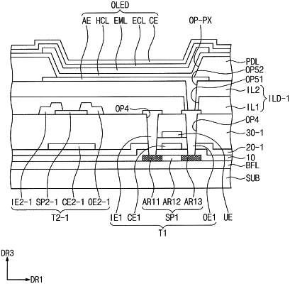
1. A semiconductor device, comprising:
a base substrate;
a first transistor disposed above the base substrate in a direction that is perpendicular to a plane of the base substrate, the first transistor comprising a connection electrode, a first output electrode, a first control electrode, and a first semiconductor pattern including a crystalline semiconductor;
a second transistor disposed above the base substrate in the direction perpendicular to the plane of the base substrate, the second transistor comprising a second input electrode, the connection electrode, a second control electrode, and a second semiconductor pattern including an oxide semiconductor;
a plurality of insulating layers disposed above the base substrate in the direction perpendicular to the plane of the base substrate; and
an upper electrode disposed above the first control electrode, in the direction perpendicular to the plane of the base substrate, with at least one insulating layer of the plurality of insulating layers interposed between the upper electrode and the first control electrode,
wherein the upper electrode at least partially overlaps the first control electrode, in the direction perpendicular to the plane of the base substrate, and forms a capacitor with the first control electrode, and
wherein the connection electrode is a single integral electrode configured as an output electrode of the second transistor and an input electrode of the first transistor.
|